Thin Film Devices Market Size, Share, Trends, Growth & Forecast 2034

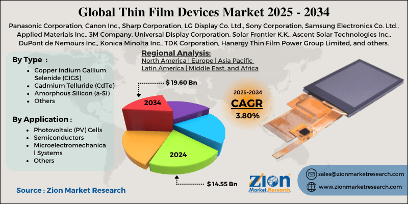
Thin Film Devices Market By Type (Copper Indium Gallium Selenide [CIGS], Cadmium Telluride [CdTe], Amorphous Silicon [a-Si], and Others), By Application (Photovoltaic [PV] Cells, Semiconductors, Microelectromechanical Systems, and Others), and By Region - Global and Regional Industry Overview, Market Intelligence, Comprehensive Analysis, Historical Data, and Forecasts 2025 - 2034
| Market Size in 2024 | Market Forecast in 2034 | CAGR (in %) | Base Year |
|---|---|---|---|
| USD 14.55 Billion | USD 19.60 Billion | 3.80% | 2024 |
Thin Film Devices Industry Perspective:
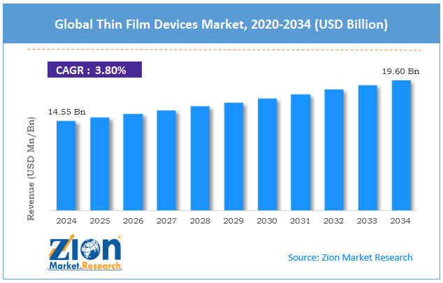
The global thin film devices market size was approximately USD 14.55 billion in 2024 and is projected to reach around USD 19.60 billion by 2034, with a compound annual growth rate (CAGR) of approximately 3.80% between 2025 and 2034.
 Request Free SampleRequest Free Sample
Key Insights:
- As per the analysis shared by our research analyst, the global thin film devices market is estimated to grow annually at a CAGR of around 3.80% over the forecast period (2025-2034)
- In terms of revenue, the global thin film devices market size was valued at around USD 14.55 billion in 2024 and is projected to reach USD 19.60 billion by 2034.
- The thin film devices market is projected to grow significantly due to the rising adoption of renewable energy technologies, advancements in thin film deposition techniques, and the expansion of flexible and wearable electronics.
- Based on type, the Cadmium Telluride (CdTe) segment is expected to lead the market, while the Copper Indium Gallium Selenide (CIGS) segment is expected to grow considerably.
- Based on application, the Photovoltaic (PV) cells segment is the largest segment, while the semiconductors segment is projected to witness substantial revenue growth over the forecast period.
- Based on region, the Asia Pacific is projected to dominate the global market during the estimated period, followed by North America.
Thin Film Devices Market: Overview
Thin film devices are advanced optical and electronic components created by depositing extremely thin layers of materials, typically ranging from nanometers to micrometers, onto a substrate. These devices are preferred due to their compact size, high efficiency, and lightweight structure. They facilitate enhanced performance in modern technologies, making them a vital part of next-generation optoelectronic and electronic advancements. The global thin film devices market is poised for significant growth, driven by the increasing adoption of renewable energy solutions, rising demand for lightweight and compact electronics, and advancements in coating and deposition technologies. Thin-film solar cells are increasingly used in renewable energy projects due to their cost-effectiveness and flexibility. Governments are offering incentives for solar adoption, thereby augmenting the deployment of thin-film technology. The worldwide installation of thin-film solar panels surged by approximately 20% in 2024, according to the IEA.
Furthermore, the miniaturization trend in electronics is driving the integration of thin films in smartphones, wearables, and displays. Their slim profile and superior electrical characteristics improve energy efficiency and device performance. Flexible displays and OLED panels rely heavily on thin-film transistors (TFTs). Advancements in CVD, ALD, and PVD have enhanced film adhesion, precision, and scalability. These solutions facilitate uniform coating at nanoscale levels, improving device yield and durability. Manufacturers are leveraging these innovations to meet high-volume production demands.
Nevertheless, the global market faces limitations due to factors such as high initial equipment and manufacturing costs, complex fabrication processes, and material sensitivity. Thin film fabrication requires advanced vacuum and deposition systems, which increase capital costs. Small companies face challenges due to high setup costs. This financial barrier restricts industry entry and worldwide competitiveness. Similarly, thin film production relies on material compatibility and precise environmental control. Minor process deviations may result in low yield rates and defects. These challenges pose operational risks and hinder industrial-scale deployment.
Still, the global thin film devices industry benefits from several favorable factors, including the growing adoption of electric vehicles and the expansion of smart glass and BIPV systems. Thin films enhance the performance of EV batteries, photovoltaic coatings, and sensors, promoting lightweight efficacy. The integration of solar films into car roofs is growing as a new design trend. The EV boom presents robust growth opportunities for thin-film applications. Additionally, thin film coatings in smart glass enhance aesthetics and energy efficiency in buildings. Building-integrated photovoltaics (BIPV) assimilate power generation with architectural design. Urban sustainability projects are fueling large-scale adoption worldwide.
Thin Film Devices Market Dynamics
Growth Drivers
How is increasing use in biosensing and medical applications fueling the thin film devices market?
Thin film technologies are becoming increasingly vital in diagnostic devices, bioelectronics, and medical sensors, as they enable precise detection and the development of miniaturized systems. For example, Abbott Laboratories and Medtronic are developing next-generation biosensing devices that employ thin film coatings for improved conductivity and biocompatibility. Recent innovations in thin-film biosensors for cardiac and glucose monitoring demonstrate growing healthcare applications. The rising intersection between biotechnology and electronics is a significant tailwind for this market.
How do improvements in thin-film deposition technologies drive the thin film devices market?
Speedy advancements in thin film deposition techniques, such as Pulsed Laser Deposition (PLD), Atomic Layer Deposition (ALD), and Sputtering, are enhancing device production and performance scalability. New systems, such as Oxford Instruments' 2025 ALD platform, enable sub-nanometer precision and energy-efficient processing. These technological improvements are reducing manufacturing costs while enhancing film adhesion and uniformity, thereby expanding the application of thin films in industries such as defense and photonics. Constant advancement in deposition is a significant growth propeller in the thin film devices market.
Restraints
Environmental and toxic material concerns negatively impact the market progress
Specific thin film devices utilize rare or toxic materials, such as tellurium (Te), cadmium (Cd), and indium (In), thereby increasing health-related and environmental risks. Improper waste management at CIGS and CdTE manufacturing plants may lead to water and soil contamination. For example, a 2025 report from Greenpeace Asia highlighted pollution issues associated with thin-film PV waste in manufacturing centers, such as those in Malaysia and China. These environmental risks are triggering stringent regulatory scrutiny, raising compliance costs for manufacturers.
Opportunities
How is the expanding role in optical coatings and photonics creating promising avenues for the thin film devices industry?
Thin films play a vital role in optical coatings, AR/VR optics, and laser systems, where they enhance reflection, transmission, and anti-reflective properties. Companies like Zeiss and Nikon are actively investing in thin film coating and high-precision facilities to support LiDAR and AR/VR technologies. The rise of immersive media, 3D sensing, and quantum optics is expected to expand the commercial potential of thin film photonics devices significantly. This increasing role ultimately fuels the growth of the thin film devices industry.
Challenges
Technical complexity and yield issues in production restrict the market growth
Manufacturing thin film devices requires sub-nanometer precision, advanced vacuum systems, and cleanroom environments, which often result in high rejection rates. According to reports, yield losses in thin-film semiconductor production may surpass 18%, especially in ALD and sputtering processes. Any slight deviation in film uniformity or thickness may result in performance degradation or device malfunction. Small firms and startups often struggle to achieve consistent product quality at scale, which hampers their commercialization. Hence, technical intricacy remains a barrier to cost efficiency and mass production.
 Request Free SampleRequest Free Sample
Thin Film Devices Market: Report Scope
| Report Attributes | Report Details |
|---|---|
| Report Name | Thin Film Devices Market |
| Market Size in 2024 | USD 14.55 Billion |
| Market Forecast in 2034 | USD 19.60 Billion |
| Growth Rate | CAGR of 3.80% |
| Number of Pages | 213 |
| Key Companies Covered | Panasonic Corporation, Canon Inc., Sharp Corporation, LG Display Co. Ltd., Sony Corporation, Samsung Electronics Co. Ltd., Applied Materials Inc., 3M Company, Universal Display Corporation, Solar Frontier K.K., Ascent Solar Technologies Inc., DuPont de Nemours Inc., Konica Minolta Inc., TDK Corporation, Hanergy Thin Film Power Group Limited, and others. |
| Segments Covered | By Type, By Application, and By Region |
| Regions Covered | North America, Europe, Asia Pacific (APAC), Latin America, Middle East, and Africa (MEA) |
| Base Year | 2024 |
| Historical Year | 2019 to 2023 |
| Forecast Year | 2025 - 2034 |
| Customization Scope | Avail customized purchase options to meet your exact research needs. Request For Customization |
Thin Film Devices Market: Segmentation
The global thin film devices market is segmented based on type, application, and region.
Based on type, the global thin film devices industry is divided into Copper Indium Gallium Selenide (CIGS), Cadmium Telluride (CdTe), Amorphous Silicon (a-Si), and others. The Cadmium Telluride (CdTe) segment holds a dominant market share, offering low manufacturing costs, high efficiency, and excellent performance in low-light conditions. This makes it the highly preferred material for large-scale solar energy projects. Its superior temperature coefficient and short energy payback time improve its suitability for utility-scale installations. Major producers, such as First Solar, continue to increase their CdTe production capacity, thereby strengthening their leadership in the global market.
Conversely, the Copper Indium Gallium Selenide (CIGS) segment held the second-largest share in the market. CIGS films offer excellent flexibility and absorption coefficients. They deliver higher efficiency than amorphous silicon and are gaining immense prominence in niche applications where flexibility and lightweight properties are vital. Constant R&D investments are enhancing CIGS scalability and yield, augmenting its rank in electronic and solar applications.
Based on application, the global thin film devices market is segmented into photovoltaic (PV) cells, semiconductors, microelectromechanical systems, and others. The photovoltaic (PV) cells segment held a dominant share in the market due to their lightweight structure, cost efficiency, and suitability for large-area solar installations. The global shift towards clean energy and government incentives for solar power adoption are driving massive investments in thin-film PV technologies. Therefore, the segment registers for the majority of thin film production and accounts for a significant portion of worldwide industry revenue.
On the other hand, the semiconductor segment held second rank, as thin film materials are increasingly used in integrated circuits, transistors, and displays to achieve miniaturization and improved performance. Their role in next-generation electronics, such as 5G chips and OLED panels, is growing rapidly. Constant innovations in nanofabrication and deposition methods are strengthening the segmental contribution in the total market expansion.
Thin Film Devices Market: Regional Analysis
What enables the Asia Pacific to have a strong foothold in the global Thin Film Devices Market?
The Asia Pacific is projected to maintain its dominant position in the global thin film devices market, driven by its strong manufacturing base and industrial infrastructure, the rapid growth in solar energy adoption, and the presence of key market players and R&D initiatives. APAC is a leader in the market due to its extensive semiconductor and electronics manufacturing base, particularly in South Korea, China, Taiwan, and Japan. These nations host prominent thin-film producers and fabrication facilities, supporting large-scale production.
Moreover, the region is experiencing significant investment in thin-film photovoltaic (PV) installations, primarily in India and China. Governments are promoting the expansion of renewable energy through the development of large-scale solar parks and incentives.
Furthermore, leading companies such as Sharp Corporation, Kaneka, and First Solar (Malaysia operations) are expanding their thin film capabilities in the region. Constant R&D efforts and collaborations between industries and universities are driving advancements in deposition technologies and materials. This infrastructure has augmented product commercialization and export competitiveness.
North America maintains its position as the second-leading region in the global thin film devices industry, driven by strong growth in solar installations and renewable energy, high demand for electronics applications and advanced semiconductors, and expanding adoption in biosensing and medical devices. The United States is the leading market for thin-film photovoltaic cells, primarily utilizing Cadmium Telluride (CdTe) technologies. Companies like First Solar, based in Arizona, are leaders in the worldwide CdTe solar market, with massive, large-scale production plants in the nation.
Moreover, the region's semiconductor industry is expanding speedily with large-scale investments in chip manufacturing and microelectronics. Thin film coatings and transistors are essential for chip packaging, device miniaturization, and 5G integration. Additionally, North America's advanced healthcare industry is incorporating thin sensors and coatings into implantables, diagnostics, and wearable health technologies. These devices reduce invasiveness, improve precision, and support real-time monitoring.
Thin Film Devices Market: Competitive Analysis
The leading players in the global thin film devices market are:
- Panasonic Corporation
- Canon Inc.
- Sharp Corporation
- LG Display Co. Ltd.
- Sony Corporation
- Samsung Electronics Co. Ltd.
- Applied Materials Inc.
- 3M Company
- Universal Display Corporation
- Solar Frontier K.K.
- Ascent Solar Technologies Inc.
- DuPont de Nemours Inc.
- Konica Minolta Inc.
- TDK Corporation
- Hanergy Thin Film Power Group Limited
Thin Film Devices Market: Key Market Trends
Rising adoption of perovskite and eco-friendly thin film materials:
A significant trend is the transition from toxic materials, such as cadmium, to high-efficiency and environmentally friendly alternatives, including copper-zinc-tin-sulfide (CZTS) and perovskite. These next-generation materials offer superior light absorption and low production costs. Worldwide R&D investment in sustainable thin film materials has increased by nearly 35% since 2022, denoting the market's green transformation.
Shift toward flexible and stretchable electronics:
The industry is experiencing strong momentum towards flexible thin film devices used in foldable smartphones, electronic textiles, and wearable sensors. Manufacturers are developing bendable thin-film transistors (TFTs) and conductive coatings to enhance durability under mechanical stress. This trend is transforming healthcare device design and consumer electronics toward adaptable and lightweight technologies.
The global thin film devices market is segmented as follows:
By Type
- Copper Indium Gallium Selenide (CIGS)
- Cadmium Telluride (CdTe)
- Amorphous Silicon (a-Si)
- Others
By Application
- Photovoltaic (PV) Cells
- Semiconductors
- Microelectromechanical Systems
- Others
By Region
- North America
- The U.S.
- Canada
- Europe
- France
- The UK
- Spain
- Germany
- Italy
- Rest of Europe
- Asia Pacific
- China
- Japan
- India
- South Korea
- Southeast Asia
- Rest of Asia Pacific
- Latin America
- Brazil
- Mexico
- Rest of Latin America
- Middle East & Africa
- GCC
- South Africa
- Rest of Middle East & Africa
Table Of Content
Methodology
FrequentlyAsked Questions
Thin film devices are advanced optical and electronic components created by depositing extremely thin layers of materials, typically ranging from nanometers to micrometers, onto a substrate. These devices are preferred due to their compact size, high efficiency, and lightweight structure.
The global thin film devices market is projected to grow due to surging demand for miniaturized electronic components, expansion of the consumer electronics industry, and demand for energy-efficient and lightweight materials.
According to study, the global thin film devices market size was worth around USD 14.55 billion in 2024 and is predicted to grow to around USD 19.60 billion by 2034.
The CAGR value of the thin film devices market is expected to be approximately 3.80% from 2025 to 2034.
Technological advancements in nanomaterials, deposition techniques, and flexible substrates are enhancing the efficiency, performance, and scalability of thin film devices across multiple industries.
Asia Pacific is expected to lead the global thin film devices market during the forecast period.
The key players profiled in the global thin film devices market include Panasonic Corporation, Canon Inc., Sharp Corporation, LG Display Co., Ltd., Sony Corporation, Samsung Electronics Co., Ltd., Applied Materials, Inc., 3M Company, Universal Display Corporation, Solar Frontier K.K., Ascent Solar Technologies, Inc., DuPont de Nemours, Inc., Konica Minolta, Inc., TDK Corporation, and Hanergy Thin Film Power Group Limited.
The competitive landscape of the thin film devices market is moderately consolidated, with leading players focusing on R&D, capacity expansion, and strategic partnerships to strengthen their global presence.
Significant investment and partnership opportunities exist in flexible electronics, the development of eco-friendly thin film materials, and large-scale collaborations in semiconductor and solar manufacturing.
The report examines key aspects of the thin film devices market, including a detailed analysis of existing growth factors and restraints, as well as an examination of future growth opportunities and challenges that will impact the market.
HappyClients