Borosilicate Glass Wafer Market Size, Share, Value and Forecast 2034

Borosilicate Glass Wafer Market By Product Type (Standard Wafers, Ultra-Thin Wafers, Thick Wafers, Custom Wafers), By Diameter (100mm, 150mm, 200mm, 300mm, and Others), By Application (Semiconductors, MEMS Devices, Optical Applications, Biotechnology, Laboratory Equipment, Consumer Electronics), By End-Use Industry (Electronics, Healthcare, Aerospace and Defense, Automotive, Research and Development), and By Region - Global and Regional Industry Overview, Market Intelligence, Comprehensive Analysis, Historical Data, and Forecasts 2025 - 2034
| Market Size in 2024 | Market Forecast in 2034 | CAGR (in %) | Base Year |
|---|---|---|---|
| USD 1.87 Billion | USD 3.52 Billion | 5.94% | 2024 |
Borosilicate Glass Wafer Industry Prospective
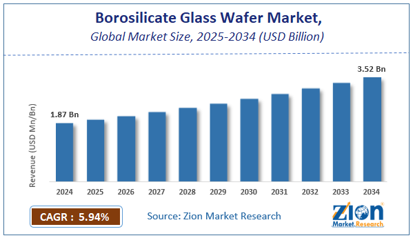
The global borosilicate glass wafer market size was worth approximately USD 1.87 billion in 2024 and is projected to grow to around USD 3.52 billion by 2034, with a compound annual growth rate (CAGR) of roughly 5.94% between 2025 and 2034.
 Request Free SampleRequest Free SampleRequest Free Sample
Key Insights
- As per the analysis shared by our research analyst, the global borosilicate glass wafer market is estimated to grow annually at a CAGR of around 5.94% over the forecast period (2025-2034).
- In terms of revenue, the global borosilicate glass wafer market size was valued at approximately USD 1.87 billion in 2024 and is projected to reach USD 3.52 billion by 2034.
- The borosilicate glass wafer market is projected to grow significantly due to expanding semiconductor production, increasing miniaturization trends in electronics, rising demand for MEMS devices, growing biotechnology research activities, and technological advancements in optical systems.
- Based on product type, the standard wafers segment is expected to lead the borosilicate glass wafer market, while the ultra-thin wafers segment is anticipated to experience significant growth.
- Based on diameter, the 200mm segment is expected to lead the borosilicate glass wafer market, while the 300mm segment is anticipated to witness notable growth.
- Based on application, the semiconductors segment is the dominating segment, while the MEMS devices segment is projected to witness sizeable revenue over the forecast period.
- Based on end-use industry, the electronics segment is expected to lead the market compared to the healthcare segment.
- Based on region, Asia Pacific is projected to dominate the global borosilicate glass wafer market during the estimated period, followed by North America.
Borosilicate Glass Wafer Market: Overview
A borosilicate glass wafer is a high-performance glass substrate used in advanced manufacturing due to its strong thermal stability, chemical resistance, and dimensional reliability. The material is produced using silicon dioxide and boron trioxide, creating a glass structure suitable for precision technology environments. Borosilicate glass wafers tolerate rapid temperature changes, harsh chemical exposure, and repeated processing cycles without surface damage or shape distortion. Standard wafer formats support common semiconductor and microelectronics production workflows. Ultra-thin borosilicate glass wafers enable compact device design, lightweight structures, and improved flexibility for miniaturized systems. Thick wafer formats offer greater mechanical strength, easier handling, and greater durability during high-stress fabrication processes. Custom borosilicate glass wafers meet specific size, thickness, and surface finish requirements for specialized projects. Semiconductor manufacturing uses borosilicate glass wafers for photolithography masks, interposers, and advanced packaging solutions.
MEMS production relies on these wafers for sensors, actuators, and microfluidic components. Optical systems benefit from high transparency and optical clarity. Biotechnology applications include diagnostic chips, microarrays, and laboratory platforms. Medical devices, research laboratories, and consumer electronics also depend on borosilicate glass wafers for reliable, precise, and long-lasting performance across critical applications. The growth of semiconductor manufacturing capacity and the increasing demand for advanced electronic devices are expected to drive expansion in the borosilicate glass wafer market throughout the forecast period.
Borosilicate Glass Wafer Market: Technology Roadmap 2025–2034
The borosilicate glass wafer market is entering a transformative development phase driven by semiconductor industry evolution, miniaturization demands, and advanced manufacturing techniques. The following is the technology roadmap divided into development phases expected to unfold through 2034.
2025–2027: Manufacturing Precision and Quality Enhancement Phase
- Advanced surface finishing improves wafer flatness to extremely fine levels, helping manufacturers achieve better accuracy and higher production yields.
- Stronger chemical strengthening methods reduce wafer breakage during handling and improve durability across multiple processing stages.
- Better glass composition improves optical clarity, supporting growing use in photonics and advanced optical device manufacturing.
2028–2031: Advanced Integration and Application Expansion Phase
- Extra-large borosilicate glass wafers above 300 mm become commercially available, supporting next-generation semiconductor production and cost efficiency.
- Special surface-coated borosilicate glass wafers gain wider use in biomedical devices, sensors, and microfluidic systems requiring functional surfaces.
2032–2034: Sustainable Innovation and Smart Manufacturing Phase
- Eco-friendly production methods use recycled materials and lower-energy consumption to reduce environmental impact across glass wafer manufacturing.
- Smart manufacturing systems apply real-time monitoring and predictive maintenance to improve consistency, reduce downtime, and control production quality.
Borosilicate Glass Wafer Market Dynamics
Growth Drivers
How is the semiconductor industry expansion increasing demand for borosilicate glass wafers?
The borosilicate glass wafer market is growing as semiconductor production increases, and companies need strong materials with high heat and chemical resistance. Semiconductor factories use borosilicate glass wafers for photomasks, interposers, and advanced packaging used in complex electronic chip designs. Photolithography uses borosilicate glass wafers because they provide stable size control and transparent surfaces for accurate nanometer-level pattern printing. Three-dimensional chip packaging increases demand by using glass interposers that provide electrical isolation, thermal management, and mechanical support for stacked chips. Compound semiconductor manufacturing for radio-frequency devices, power electronics, and optoelectronic parts supports growth using borosilicate glass substrates with reliable insulating properties. MEMS manufacturing relies on borosilicate glass wafers for sensors, microfluidic channels, and actuators that require smooth, consistent surface quality.
Advanced packaging methods such as fan-out wafer-level packaging and through-glass via technology support steady long-term demand. Memory chips, logic processors, artificial intelligence accelerators, display driver chips, and sensor interface devices together increase global use of borosilicate glass wafers.
Consumer electronics proliferation creates expanding opportunities.
The global borosilicate glass wafer market is growing as demand for consumer electronics, including smartphones, tablets, wearables, and smart home devices, rises worldwide. Smartphone manufacturing creates a strong demand for borosilicate glass wafers used in fingerprint, proximity, and light sensors, as well as camera modules. Wearable device production, such as smartwatches and fitness trackers, supports market growth by enabling the integration of compact sensors onto chemically resistant glass substrates. Wireless earbuds and audio accessories rely on MEMS microphones produced on borosilicate glass wafers, offering stable acoustic and performance characteristics. Smart home devices, including voice assistants, security cameras, and environmental sensors, drive a steady demand for reliable, high-quality glass wafer materials. Augmented and virtual reality headsets use optical components and displays fabricated from borosilicate glass wafers to enhance clarity. The growth of automotive electronics, driven by driver assistance systems, infotainment screens, and sensor arrays, increases demand for specialized borosilicate glass substrates.
Restraints
How are high manufacturing costs and technical complexity limit market accessibility ?
A major challenge in the borosilicate glass wafer market is the high capital requirements, which create strong entry barriers for new and smaller manufacturers. Production relies on specialized high-temperature melting furnaces, large-scale production, careful thermal control, and stable, continuous operation. Advanced grinding and polishing equipment needed to meet strict surface flatness standards requires significant upfront investment for borosilicate glass wafer producers. Quality control systems, including optical inspection tools, surface measurement equipment, and defect detection systems, add high recurring operating expenses. Chemical processing facilities for cleaning, surface treatment, and etching need large infrastructure investment and strict regulatory compliance management. Manufacturing operations require skilled technicians who can operate complex equipment while maintaining consistent borosilicate glass wafer quality. High-purity raw materials carry premium costs, while waste management and environmental compliance systems increase ongoing operational expenses.
Opportunities
How is the advancement of biotechnology creating growth potential for the borosilicate glass wafer market?
The borosilicate glass wafer industry offers strong growth opportunities as biotechnology research and medical diagnostics expand worldwide, driving demand for safe, biocompatible substrate materials. Microarray technology development supports market growth by using glass substrates for DNA sequencing, protein testing, gene expression studies, and biomedical research work. Lab-on-a-chip diagnostic devices rely on borosilicate glass wafers because they offer clear optical performance and strong chemical resistance, enabling precise microfluidic channel fabrication. Cell culture activities in pharmaceutical research and regenerative medicine depend on glass substrates that provide biocompatible surfaces and reliable sterility.
Biosensor development for medical monitoring, environmental analysis, and food safety testing creates additional demand for functionalized borosilicate glass wafer products. Organ-on-a-chip platforms for drug discovery use borosilicate glass to support controlled microenvironments and realistic simulation of biological processes. High-throughput screening systems in pharmaceutical discovery require glass wafer substrates for automated liquid handling and optical detection accuracy. Tissue engineering, immunoassay platforms, digital pathology systems, and spatial biology analysis tools further strengthen long-term growth across global biotechnology and life science sectors.
Challenges
How are alternative substrate materials and competition creating obstacles for the borosilicate glass wafer industry?
The borosilicate glass wafer industry faces strong competition from alternative substrate materials, including silicon, sapphire, advanced polymers, ceramics, and compound semiconductor platforms. Silicon wafer technology dominates semiconductor manufacturing through mature supply chains, standardized processes, broad equipment compatibility, and large-scale production efficiencies. Sapphire substrates are gaining adoption in LED production, high-frequency electronics, and optical systems due to their hardness and thermal performance. Advanced polymer substrates challenge glass wafers in flexible electronics, wearable devices, and lightweight designs that require bending tolerance and reduced mass.
Silicon carbide and gallium nitride substrates compete in power electronics and high-temperature applications due to their superior electrical and thermal characteristics. Fused silica, quartz, and ceramic substrates serve niche roles in optics and high-temperature electronics, each with distinct expansion and durability profiles. Cost pressure from large silicon wafer suppliers, driven by economies of scale, creates pricing challenges for borosilicate glass wafer producers. Brittleness, lower thermal conductivity, limited electrical routing, and customer preference for silicon processes are restricting the borosilicate glass wafer market.
 Request Free SampleRequest Free SampleRequest Free Sample
Borosilicate Glass Wafer Market : Report Scope
| Report Attributes | Report Details |
|---|---|
| Report Name | Borosilicate Glass Wafer Market Research Report |
| Market Size in 2024 | USD 1.87 Billion |
| Market Forecast in 2034 | USD 3.52 Billion |
| Growth Rate | CAGR of 5.94% |
| Number of Pages | 220 |
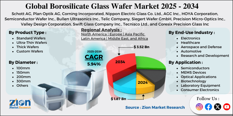
| Key Companies Covered | Schott AG, Plan Optik AG, Corning Incorporated, Nippon Electric Glass Co. Ltd., AGC Inc., HOYA Corporation, Semiconductor Wafer Inc., Bullen Ultrasonics Inc., Telic Company, Siegert Wafer GmbH, Precision Micro-Optics Inc., Valley Design Corporation, Swift Glass Company Inc., Tecnisco Ltd., and Coresix Precision Glass Inc |
| Segments Covered | By Product Type, By Diameter, By Application, By End-Use Industry, And By Region |
| Regions Covered | North America, Europe, Asia Pacific (APAC), Latin America, The Middle East and Africa (MEA) |
| Base Year | 2024 |
| Historical Year | 2019 to 2023 |
| Forecast Year | 2025 - 2034 |
| Customization Scope | Avail customized purchase options to meet your exact research needs. Request For Customization |
Borosilicate Glass Wafer Market: Segmentation
The global borosilicate glass wafer market is segmented based on product type, diameter, application, end-use industry, and region.
Based on product type, the global borosilicate glass wafer industry is classified into standard, ultra-thin, thick, and custom wafers. Standard wafers lead the market due to widespread adoption across mainstream semiconductor and MEMS applications and established manufacturing processes that support high-volume production.
Based on diameter, the industry is divided into 100mm, 150mm, 200mm, 300mm, and others. The 200mm segment leads the market due to an optimal balance between production costs and application versatility, compatibility with an extensive installed base of manufacturing equipment, and strong demand from MEMS and specialty semiconductor producers.
Based on application, the global borosilicate glass wafer market is segregated into semiconductors, MEMS devices, optical applications, biotechnology, laboratory equipment, and consumer electronics. Semiconductors are expected to lead the market during the forecast period due to continuous capacity expansion in global fabrication facilities and sustained technological advancement driving component miniaturization.
Based on end-use industry, the global market is divided into electronics, healthcare, aerospace and defense, automotive, and research and development. Electronics holds the largest market share due to massive production volumes in consumer devices, sustained innovation in semiconductor technology, and continuous growth in global electronics manufacturing output.
Borosilicate Glass Wafer Market: Regional Analysis
What factors are contributing to the Asia Pacific's dominance in the global borosilicate glass wafer market?
Asia Pacific is projected to grow at nearly 7.8 percent CAGR, maintaining leadership in the global borosilicate glass wafer market during the forecast period. The region leads the borosilicate glass wafer market because of strong semiconductor manufacturing capacity, large electronics production bases, supportive government policies, and competitive manufacturing costs. China drives regional demand through fast semiconductor factory expansion, high investment in domestic chip manufacturing, and national technology self-sufficiency programs. Taiwan holds an important role through advanced foundry operations, high-end packaging facilities, and strong expertise in semiconductor process engineering. South Korea supports market growth through large-scale memory chip manufacturing, display panel production, and high-volume consumer electronics manufacturing activities.
Japan contributes steady demand through precision electronics manufacturing, advanced materials development, sensor technology leadership, and a well-developed glass processing industry. Singapore strengthens regional growth through semiconductor assembly services, testing operations, research centers, and a strong presence of global technology headquarters. Malaysia, Thailand, and Vietnam expand demand through rising electronics manufacturing, increased foreign direct investment, and growing semiconductor assembly ecosystems. India shows emerging potential through electronics manufacturing incentives, expanding semiconductor design capabilities, and rising domestic consumer electronics production volumes. Strong supply chain integration, efficient logistics networks, a skilled technical workforce, and proximity to major end-use markets support regional dominance. Ongoing technology transfer, regional research collaboration, and continuous capacity expansion reinforce Asia Pacific leadership in the global borosilicate glass wafer market.
Government-backed semiconductor incentive programs across multiple Asia-Pacific countries continue to attract global manufacturers and expand borosilicate glass wafer production capacity. Rising investment in advanced packaging, MEMS fabrication, and sensor manufacturing increases long-term demand for high-quality borosilicate glass wafers. Expanding domestic electronics consumption, combined with export-focused manufacturing strategies, further strengthens Asia Pacific leadership in the global borosilicate glass wafer market.
North America maintains a significant market share.
North America is projected to grow at a 5.2 percent CAGR, remaining the second largest region in the global borosilicate glass wafer market. The region holds a strong position due to advanced semiconductor research, a large biotechnology presence, strong intellectual property protection, and high government technology funding. The United States drives demand through leading semiconductor companies, wide MEMS development, major biotechnology centers, and large defense electronics needs. Silicon Valley supports market growth through sustained innovation in consumer electronics, advanced sensor design, startup growth, and early adoption of new technologies. Medical device manufacturing creates steady demand for biocompatible borosilicate glass wafers used in diagnostic equipment, implantable devices, and laboratory instruments. Defense and aerospace sectors require specialized glass wafers for military electronics, satellite systems, navigation equipment, and high-reliability sensor applications. Biotechnology hubs in Boston, San Diego, and San Francisco increase consumption through pharmaceutical research, genetic testing, and the development of diagnostic platforms.
Canada supports growth through telecommunications equipment manufacturing, photonics research programs, specialty glass production, and collaborative innovation initiatives and networks. Mexico supports regional demand through expansion of electronics assembly, automotive sensor manufacturing, growth in medical device production, and export-oriented supply chains. Strong intellectual property systems, industry-academia collaboration, advanced manufacturing capacity, venture capital funding, reshoring incentives, and supply chain resilience support growth. Government incentives for domestic semiconductor production and the commercialization of research improve the long-term prospects for the North American borosilicate glass wafer market.
Recent Developments
- In September 2025, SCHOTT AG showcased new high-performance specialty glass carrier wafers and precision-engineered glass panels for advanced semiconductor packaging at SEMICON Taiwan 2025, while accelerating expansion of global production capabilities to meet rising demand from advanced packaging and high-performance computing sectors.
- In December 2025, Nippon Electric Glass Co., Ltd announced plans to begin the world’s first mass production of low-carbon pharmaceutical-grade borosilicate glass tubing using an all-electric melting furnace at its Selangor, Malaysia facility, targeting a reduction in CO₂ emissions up to 90 percent and responding to global sustainability demands from pharmaceutical and medical packaging customers.
Borosilicate Glass Wafer Market: Competitive Analysis
The leading players in the global borosilicate glass wafer market are
- Schott AG
- Plan Optik AG
- Corning Incorporated
- Nippon Electric Glass Co Ltd
- AGC Inc
- HOYA Corporation
- Semiconductor Wafer Inc
- Bullen Ultrasonics Inc.
- Telic Company
- Siegert Wafer GmbH
- Precision Micro-Optics Inc
- Valley Design Corporation
- Swift Glass Company Inc
- Tecnisco Ltd
- Coresix Precision Glass Inc
The global borosilicate glass wafer market is segmented as follows:
By Product Type
- Standard Wafers
- Ultra-Thin Wafers
- Thick Wafers
- Custom Wafers
By Diameter
- 100mm
- 150mm
- 200mm
- 300mm
- Others
By Application
- Semiconductors
- MEMS Devices
- Optical Applications
- Biotechnology
- Laboratory Equipment
- Consumer Electronics
By End-Use Industry
- Electronics
- Healthcare
- Aerospace and Defense
- Automotive
- Research and Development
By Region
- North America
- The U.S.
- Canada
- Europe
- France
- The UK
- Spain
- Germany
- Italy
- Rest of Europe
- Asia Pacific
- China
- Japan
- India
- South Korea
- Southeast Asia
- Rest of Asia Pacific
- Latin America
- Brazil
- Mexico
- Rest of Latin America
- Middle East & Africa
- GCC
- South Africa
- Rest of Middle East & Africa
Table Of Content
Methodology
FrequentlyAsked Questions
HappyClients