Advanced Semiconductor Packaging Market Size & Forecast 2034

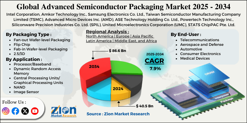
Advanced Semiconductor Packaging Market By Packaging Type (Fan-out Wafer-level Packaging, Flip Chip, Fab-in Wafer-level Packaging, and 2.5/3D), By Application (Processor/Baseband, Dynamic Random Access Memory, Central Processing Units/Graphical Processing Units, NAND, Image Sensor, and Others), By End-User (Telecommunications, Aerospace and Defense, Automotive, Consumer Electronics, Medical Devices, and Others), and By Region - Global and Regional Industry Overview, Market Intelligence, Comprehensive Analysis, Historical Data, and Forecasts 2025 - 2034
| Market Size in 2024 | Market Forecast in 2034 | CAGR (in %) | Base Year |
|---|---|---|---|
| USD 40.5 Billion | USD 86.6 Billion | 7.9% | 2024 |
Advanced Semiconductor Packaging Industry Prospective
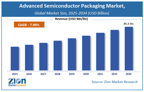
The global advanced semiconductor packaging market size was worth around USD 40.5 billion in 2024 and is predicted to grow to around USD 86.6 billion by 2034, with a compound annual growth rate (CAGR) of roughly 7.9% between 2025 and 2034.
Key Insights
- As per the analysis shared by our research analyst, the global advanced semiconductor packaging market is estimated to grow annually at a CAGR of around 7.9% over the forecast period (2025-2034).
- In terms of revenue, the global advanced semiconductor packaging market size was valued at around USD 40.5 billion in 2024 and is projected to reach USD 86.6 billion by 2034.
- Growing consumer electronics sector is expected to drive the advanced semiconductor packaging market over the forecast period.
- Based on the packaging type, the flip chip segment is expected to dominate the market over the projected period.
- Based on the application, the central processing units/graphical processing units segment is expected to capture the largest market share over the projected period.
- Based on the end-user, the consumer electronics segment is expected to capture the largest market share over the projected period.
- Based on region, the Asia Pacific is expected to dominate the market during the forecast period.
Advanced Semiconductor Packaging Market: Overview
Advanced semiconductor packaging employs several next-generation technologies for encapsulating, interconnecting, and integrating semiconductor devices that exceed those of traditional wire-bond and lead-frame packaging. It lets it put numerous dies, like logic, memory, analog, and RF, into one package using methods like 2.5D and 3D integration, fan-out wafer-level packaging (FOWLP), flip-chip, system-in-package (SiP), and chiplet architecture. These technologies greatly improve electrical performance, power efficiency, bandwidth, and thermal management while reducing the form factor.
Advanced semiconductor packaging has become an important part of modern applications like artificial intelligence (AI), high-performance computing (HPC), 5G/6G communications, automotive electronics, and advanced consumer devices. This is especially true as scaling traditional transistors becomes harder and more expensive.
Advanced Semiconductor Packaging Market Dynamics
Growth Drivers
Why does the growth in automotive electronics and autonomous systems propel the advanced semiconductor packaging industry?
The demand for advanced semiconductor packaging is expanding as cars get more electronics and self-driving systems. Modern cars need semiconductor solutions that are fast, small, and reliable. They require chips that can handle large data volumes with low latency and operate reliably under harsh conditions, such as high temperatures and vibration, and that have long lifetimes, for advanced driver-assistance systems (ADAS), autonomous driving platforms, electric vehicle (EV) powertrains, infotainment systems, and vehicle-to-everything (V2X) communication. Advanced packaging technologies, including system-in-package (SiP), 2.5D/3D integration, and high-density interconnects, enable adding more features to smaller spaces while improving thermal performance, signal integrity, and durability. As more car companies adopt software-defined vehicles and more self-driving cars hit the road, the need for improved semiconductor packaging intensifies. This helps the advanced semiconductor packaging market expand in the long run.
Restraints
How does the high manufacturing cost impede the growth of the advanced semiconductor packaging industry?
The high manufacturing costs are among the most significant reasons for the advanced semiconductor packaging market processes are not developing well. This is because such technologies involve complicated manufacturing, the use of expensive materials, and the need for high-end tools. Applications requiring such precision, such as 2.5D and 3D IC packaging, fan-out wafer-level, and chiplet integration, not only require high-end lithography but also top-class substrates, interposers, and complex thermal control, all of which increase capital and operational costs. Further, low initial yields, strict quality norms, and testing as a must-have together lead to high production costs. These high costs might prevent price-sensitive markets or small companies from adopting the technology, thus preventing advanced semiconductor packaging solutions with their excellent performance from reaching the world as a selling point.
Opportunities
Does the growing collaboration offer a potential opportunity for the advanced semiconductor packaging industry?
The increasing collaboration of market players with science agencies is expected to foster the market growth over the analysis period. For instance, in May 2025, GlobalFoundries, through its newly signed Memorandum of Understanding (MOU) with the Agency for Science, Technology, and Research (A*STAR), announced its intention to further its advanced packaging capabilities. A*STAR is the leading public sector research and development (R&D) agency of Singapore. Advanced packaging is a significant R&D priority in the semiconductor industry and will remain so, primarily due to the growing demand for AI and other data-intensive applications, including high-performance computing, data centers, and 5G/6G communications.
The industry will require miniaturized, high-performance, energy-efficient technology solutions that advanced packaging technologies will deliver to drive long-term growth. Under the MOU terms, A*STAR will allow GF to use its R&D facilities, capabilities, and tech support, while GF will give A*STAR the vital equipment to advance its R&D efforts. The partnership will accelerate GF's plans to develop and commercialize its advanced packaging solutions and broaden its services to provide clients with a single source for semiconductor chips fabricated, processed, packaged, and tested at GF’s Singapore manufacturing site.
Challenges
How does the shortage of skilled workforce challenge market expansion?
The absence of a proficient workforce presents a serious obstacle to the expansion of the advanced semiconductor packaging market, as such technologies require a highly specialized, trained workforce with knowledge in heterogeneous integration, wafer-level processing, thermal management, and reliability testing. Modern packaging methods are more intricate than existing ones, necessitating the presence of highly skilled engineers and well-trained staff to maintain precision, yield, and quality. The relentless shortage of such qualified personnel turns the production ramp-up strategy into a much longer process, and it also increases the costs of labor.
The risk of errors during manufacturing is also heightened; together, these factors limit the range and slow the adoption of advanced packaging solutions across industries such as automotive, AI, and high-performance computing, which typically involve high-tech products. For instance, according to the SEMI, the industry will require a global workforce that consists of 1 million skilled workers by 2030, with Europe having a deficit of over 100,000 engineers and Asia-Pacific having more than 200,000. This growth implies the need for at least 100,000 second-line leaders and 10,000 third-line leaders—most of whom must be sourced from outside the industry.
Advanced Semiconductor Packaging Market : Report Scope
| Report Attributes | Report Details |
|---|---|
| Report Name | Advanced Semiconductor Packaging Market Research Report |
| Market Size in 2024 | USD 40.5 Billion |
| Market Forecast in 2034 | USD 86.6 Billion |
| Growth Rate | CAGR of 7.9% |
| Number of Pages | 220 |
| Key Companies Covered | Intel Corporation, Amkor Technology Inc., Samsung Electronics Co. Ltd., Taiwan Semiconductor Manufacturing Company Limited (TSMC), Advanced Micro Devices Inc. (AMD), ASE Technology Holding Co. Ltd., Powertech Technology Inc., Siliconware Precision Industries Co. Ltd. (SPIL), United Microelectronics Corporation (UMC), STATS ChipPAC Pte. Ltd., ChipMOS Technologies Inc., Texas Instruments Incorporated, Broadcom Inc., NXP Semiconductors N.V., and Micron Technology Inc |
| Segments Covered | By Packaging Type, By Application, By End-User, And By Region |
| Regions Covered | North America, Europe, Asia Pacific (APAC), Latin America, The Middle East and Africa (MEA) |
| Base Year | 2024 |
| Historical Year | 2019 to 2023 |
| Forecast Year | 2025 - 2034 |
| Customization Scope | Avail customized purchase options to meet your exact research needs. Request For Customization |
Advanced Semiconductor Packaging Market: Segmentation
By Packaging Type, The flip chip segment is expected to dominate the market. The segment's growth can be attributed to its ability to deliver improved electrical performance, higher input/output (I/O) density, and superior thermal management compared with conventional wire-bond packaging. Through flip-chip technology, direct solder bumps between the chip and substrate provide shorter signal paths, less power loss, and increased operating speeds. The advantages mentioned above make flip-chip packaging very appropriate for high-performance applications like AI processors, high-performance computing (HPC), data centers, 5G infrastructure, and advanced automotive electronics.
By Application, The central processing units/graphical processing units segment is expected to hold the largest revenue share over the projected period. The growing market is mainly driven by the super-high demand for high-performance computing in data centers, AI, machine learning, cloud computing, and high-end graphics applications, which will soon be the major users of the spectrum. The high-performance requirements of today's CPUs and GPUs, including very high bandwidth, very low latency, and efficient power and thermal management, cannot be met by conventional packaging solutions.
Advanced packaging technologies such as flip-chip, 2.5D/3D IC integration, chiplet-based architectures, and HBM integration are enabling higher I/O density, faster data transfer, and improved heat dissipation. The increasing application of AI, real-time data analytics, and high-performance computing in both enterprise and consumer markets is a major factor driving the adoption of advanced packaging for CPUs and GPUs, and consequently, overall market revenue growth.
By End-User, The consumer electronics segment is expected to grow substantially over the forecast period. The primary driver of the market's expansion is the need for small, light, and powerful electronic devices. Among the electronics, smartphones, tablets, wearables, and smart home devices are those that require high levels of integration, improved performance, and low power consumption in small form factors. Cutting-edge packaging techniques, such as flip-chip, fan-out wafer-level packaging (FOWLP), and system-in-package (SiP), enable multiple functions to be integrated into a single package while maintaining signal integrity, thermal performance, and battery efficiency.
Additionally, consumers are highly discerning and expect every product to offer fast connectivity and advanced graphics; thus, the use of advanced semiconductor packaging in consumer electronics is the primary driver of sustained market revenue growth and, consequently, the device upgrade cycle, 5G adoption, and related trends.
Advanced Semiconductor Packaging Market: Regional Analysis
Why does the Asia Pacific dominate the advanced semiconductor packaging market?
Asia-Pacific has been the largest contributor to the advanced semiconductor packaging market in terms of both volume and revenue growth, due to its dominance in semiconductor manufacturing and packaging worldwide. In leading countries such as China, Taiwan, South Korea, and Japan, there is a massive presence of foundries, OSATs, and electronics manufacturers. The presence of all these players in one place has made it easier and more cost-effective to implement advanced packaging technologies. The area is well-positioned to produce at very large scales, with the best-trained workers in manufacturing, and to meet consumer demand in the cushioning industries of electronics, automotive electronics, and related sectors, including 5G and data centers.
Moreover, investments in advanced packaging plants are on the rise, governments are supporting semiconductor self-sufficiency, and the rapid adoption of applications such as AI, high-performance computing, and electric vehicles is accelerating developments in the region. Therefore, the Asia Pacific region is still the leader in both volume and revenue growth in the advanced semiconductor packaging sector.
Advanced Semiconductor Packaging Market: Competitive Analysis
The global advanced semiconductor packaging market is dominated by players like
- Intel Corporation
- Amkor Technology Inc
- Samsung Electronics Co Ltd
- Taiwan Semiconductor Manufacturing Company Limited (TSMC)
- Advanced Micro Devices Inc (AMD)
- ASE Technology Holding Co Ltd
- Powertech Technology Inc
- Siliconware Precision Industries Co Ltd (SPIL)
- United Microelectronics Corporation (UMC)
- STATS ChipPAC Pte Ltd
- ChipMOS Technologies Inc
- Texas Instruments Incorporated
- Broadcom Inc
- NXP Semiconductors N V
- Micron Technology Inc
The global advanced semiconductor packaging market is segmented as follows:
By Packaging Type
- Fan-out Wafer-level Packaging
- Flip Chip
- Fab-in Wafer-level Packaging
- 2.5/3D
By Application
- Processor/Baseband
- Dynamic Random Access Memory
- Central Processing Units/ Graphical Processing Units
- NAND
- Image Sensor
- Others
By End-User
- Telecommunications
- Aerospace and Defense
- Automotive
- Consumer Electronics
- Medical Devices
- Others
By Region
- North America
- The U.S.
- Canada
- Europe
- France
- The UK
- Spain
- Germany
- Italy
- Rest of Europe
- Asia Pacific
- China
- Japan
- India
- South Korea
- Southeast Asia
- Rest of Asia Pacific
- Latin America
- Brazil
- Mexico
- Rest of Latin America
- Middle East & Africa
- GCC
- South Africa
- Rest of Middle East & Africa
Table Of Content
Methodology
FrequentlyAsked Questions
What are the major challenges restraining the growth of the advanced semiconductor packaging market?
HappyClients