Semiconductor Bonding Market Size, Share, Trends, Growth 2034

Semiconductor Bonding Market By Type (Die Bonder, Wafer Bonder, Flip Chip Bonder), By Proces Type (Die To Die Bonding, Die To Wafer Bonding, Wafer To Wafer Bonding), By Bonding Technology (Die Bonding Technology, Wafer Bonding Technology, Wafer Bonding Technology, Direct and Anodic Wafer Bonding, Indirect Wafer Bonding), By Application (RF Devices, Mems and Sensors, CMOS Image Sensors, LED, 3D NAND), and By Region: Global and Regional Industry Overview, Market Intelligence, Comprehensive Analysis, Historical Data, and Forecasts 2025 - 2034
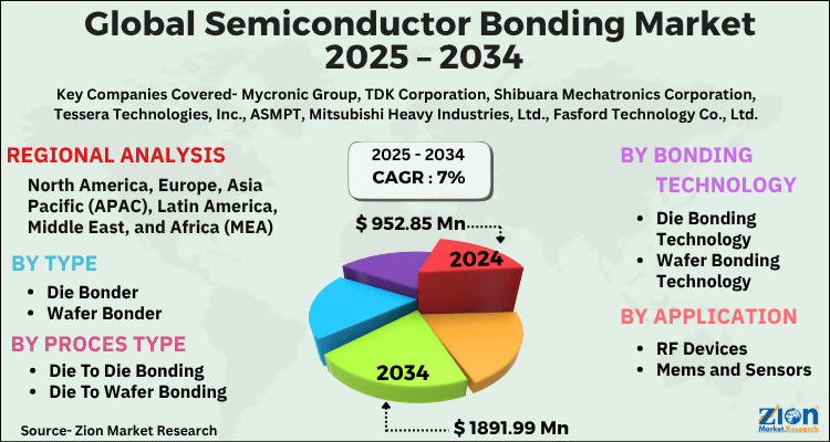
| Market Size in 2024 | Market Forecast in 2034 | CAGR (in %) | Base Year |
|---|---|---|---|
| USD 952.85 Million | USD 1891.99 Million | 7% | 2024 |
Semiconductor Bonding Market: Industry Perspective
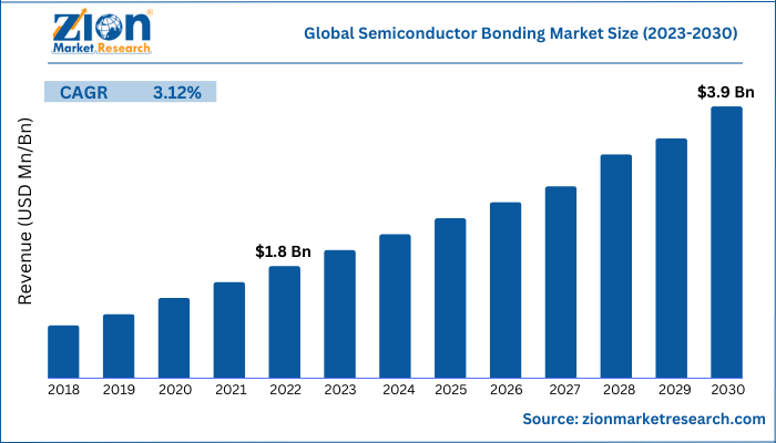
The global semiconductor bonding market size was worth around USD 952.85 Million in 2024 and is predicted to grow to around USD 1891.99 Million by 2034 with a compound annual growth rate (CAGR) of roughly 7% between 2025 and 2034. The report analyzes the global semiconductor bonding market's drivers, restraints/challenges, and the effect they have on the demands during the projection period. In addition, the report explores emerging opportunities in the semiconductor bonding industry.
Global Semiconductor Bonding Market: Synopsis
Semiconductor is a material possessing electrical conductivity. Moreover, the semiconductor arrangement of atoms is in the form of a homogeneous structure and the model of semiconductor bonding is used in producing a large number of fabrication equipment and many integrated circuits. Furthermore, semiconductors can either be molecules such as gallium arsenide or silicon. Rising demand for stacked die systems in IoT equipment and escalating popularity of hybrid and electric vehicles have enhanced the popularity of semiconductor bonding in recent years. Furthermore, semiconductor, which is also referred to as integrated circuit, boost the digital economy. Comprising a large number of miniature electronic components connected together, semiconductors are known as the brains of modern electronic devices such as televisions, tablets, smartphones, and laptops.
Key Insights
- As per the analysis shared by our research analyst, the global semiconductor bonding market is estimated to grow annually at a CAGR of around 7% over the forecast period (2025-2034).
- Regarding revenue, the global semiconductor bonding market size was valued at around USD 952.85 Million in 2024 and is projected to reach USD 1891.99 Million by 2034.
- The semiconductor bonding market is projected to grow at a significant rate due to rising demand for advanced packaging in electronics, increasing miniaturization of devices, growth in automotive and IoT applications, and advancements in heterogeneous integration technologies.
- Based on Type, the Die Bonder segment is expected to lead the global market.
- On the basis of Proces Type, the Die To Die Bonding segment is growing at a high rate and will continue to dominate the global market.
- Based on the Bonding Technology, the Die Bonding Technology segment is projected to swipe the largest market share.
- By Application, the RF Devices segment is expected to dominate the global market.
- Based on region, Asia-Pacific is predicted to dominate the global market during the forecast period.
Semiconductor Bonding Market: Growth Factors
Large-scale penetration of semiconductor bonding equipment in consumer electronic goods, aerospace, and medical sectors to boost the global market trends
A tremendous growth witnessed in the electronics sector in the last few decades is related to the declining costs of semiconductors and a function of Moore’s law. This has boosted the demand for semiconductors in the electronics sector, thereby charting a profitable growth map for the global semiconductor bonding market. Emergence of new technologies such as artificial intelligence, power-efficient sensing devices, brain-inspired computing, robotics, and automated equipment has contributed sizably towards the global market surge. Moreover, semiconductor bonding is very complex and it finds application in consumer electronics products, computing & communication equipment, aerospace, medical, retail, and aerospace sectors.
Some of the semiconductor firms with extensive value & supply chains and a strong ecosystem across the globe will boost the global semiconductor bonding market trends. For instance, the U.S. semiconductor firm has more than 16.050 suppliers globally. For the record, over 7,500 of its semiconductor suppliers are based in nearly 46 various states in the U.S. and nearly over 8,600 suppliers of semiconductors are outside the U.S.
Semiconductor Bonding Market: Hindrances
Massive costs of ownership of semiconductor bonding equipment to put brakes on the global industry surge
Huge ownership costs and the cost of producing semiconductor bonding devices are likely to inhibit the expansion of the global semiconductor bonding industry. Furthermore, assembling of various big and small components including sensors, screens, and vacuum can further hinder the growth of the global industry.
Semiconductor Bonding Market: Opportunities
Escalating popularity of 3D semiconductor assembling to open new growth opportunities for the global market
Surging popularity of 3D semiconductor assembling and the thriving packaging sector as well as the use of connected things and machine learning tools in a spectrum of industries will create new growth avenues for the global semiconductor bonding market size.
Semiconductor Bonding Market: Challenges
Volatility of thin wafers and imbalance of moving parts of semiconductor bonding devices create new challenges for the industry growth globally
Volatility of thin wafers and their damage susceptibility due to outside stress or pressure can be a major challenge in the growth path of the global semiconductor bonding industry. Furthermore, an imbalance of moving components of semiconductor bonding can pose a major challenge in the growth path of the global industry.
Semiconductor Bonding Market: Segmentation
The global semiconductor bonding market is sectored into type, process type, application, bonding technology, and region.
In terms of type, the global semiconductor bonding market is sectored into flip chip bonder, die bonder, and wafer bonder segments. Apparently, the wafer bonder segment, which lead the global market share in 2022, is set to continue its overall market domination over the forecast timeline. The segmental surge can be credited to the ability of the wafer bonder to accurately preserve the orientation between the two bonded surfaces of the semiconductor.
Based on the application, the global semiconductor bonding industry is bifurcated into CMOS image sensors, 3D NAND, RF devices, LED, and MEMS & sensors segments. Furthermore, the LED segment, which garnered the largest share of the global industry in 2022, will continue to dominate the global industry share even in near future. The growth of the segment over the assessment period can be due to the ability of LED in consuming less power & low heat emission. Apart from this, its eco-friendly nature has enhanced its popularity across the globe.
On basis of bonding technology, the semiconductor bonding market across the globe is segmented into wafer bonding technology and die bonding technology segments. Reportedly, the die bonding technology segment, which led the technology domain in 2022, is projected to continue its segmental domination even in the near future. The segmental expansion over 2023-2030 can be attributed to the high durability offered by die bonding technology in semiconductor bonding.
Recent Breakthroughs
- In the first half of 2020, GlobalWafers Company Limited, a Taiwanese tech manufacturing firm, invested nearly $339.1 million in expanding the production capacity of its silicon wafer unit set up in Taisil, Taiwan. The move is aimed at increasing the demand for silicon wafers in the country and across the globe.
- In August 2020, HANMI Semiconductor, a semiconductor firm based in South Korea that manufactures semiconductor equipment, launched a new flip chip bonder 5.0. The strategic move is aimed at increasing the production of semiconductors in South Korea. The initiative will increase the demand for semiconductor bonding equipment in South Korea & Asia-Pacific region. Apart from this, it will provide impetus to the growth of the semiconductor bonding business in the Asian sub-continent.
Semiconductor Bonding Market: Report Scope
| Report Attributes | Report Details |
|---|---|
| Report Name | Semiconductor Bonding Market |
| Market Size in 2024 | USD 952.85 Million |
| Market Forecast in 2034 | USD 1891.99 Million |
| Growth Rate | CAGR of 7% |
| Number of Pages | 202 |
| Key Companies Covered | Mycronic Group, TDK Corporation, Shibuara Mechatronics Corporation, Tessera Technologies, Inc., ASMPT, Mitsubishi Heavy Industries, Ltd., Fasford Technology Co., Ltd., Sky Water Technology, Intel Corporation, Kulicke and Soffa Industries, EV Group (EVG), SHINKAWA Electric Co., Ltd, Besemiconductor, Palomar Technologies, Panasonic Corporation, SUSS MicroTec SE, Tokyo Electron Limited, and others. |
| Segments Covered | By Type, By Proces Type, By Bonding Technology, By Application, and By Region |
| Regions Covered | North America, Europe, Asia Pacific (APAC), Latin America, The Middle East and Africa (MEA) |
| Base Year | 2024 |
| Historical Year | 2020 to 2023 |
| Forecast Year | 2025 - 2034 |
| Customization Scope | Avail customized purchase options to meet your exact research needs. Request For Customization |
Semiconductor Bonding Market: Regional Insights
Semiconductor Bonding Market in the Asia-Pacific Zone To Record the Fastest CAGR In 2025 - 2034
The Asia-Pacific semiconductor bonding market is projected to register the highest growth rate over the forecasting timeframe. The regional market growth over 2025 - 2034 can be ascribed to China, Taiwan, and South Korea being the world’s leading manufacturers of semiconductors. In addition to this, the presence of key manufacturers in the region will account notably toward the regional market growth in the upcoming years.
The North American region, which contributed a major share of the overall semiconductor bonding industry in 2022, is set to maintain its market domination during the forecast timeline. The growth of the regional market in forecasting years can be owing to escalating demand for 3D semiconductor assembly and packaging solutions in the countries such as the U.S. and Canada. Moreover, the rise in the adoption of IoT, sensing technology, and AI in the region will proliferate the size of the semiconductor bonding industry in North America.
Semiconductor Bonding Market: Competitive Analysis
The report provides a company market share analysis to give a broader overview of the key market players. In addition, the report also covers key strategic developments of the market, including acquisitions & mergers, new product launches, agreements, partnerships, collaborations & joint ventures, research & development, and regional expansion of major participants involved in the semiconductor bonding market on a global and regional basis.
The global semiconductor bonding industry profiles key players such as:
- Kulicke & Soffa
- Moschip Technologies Ltd
- Tata Elxsi Ltd
- Shinkawa Ltd
- Shibaura Mechatronics
- Yamaha Motor Robotics Corporation Co.
- Fuji Corporation
- SPEL Semiconductor Ltd
- Panasonic Corporation
- SUSS MicroTech SE
- ASM Pacific Technology Ltd.
- Fasford Technology
- EV Group
- Ruttonsha International Rectifier Ltd
- Dixon Technologies (India) Ltd
- BE Semiconductor Industries N.V.
The global semiconductor bonding market is segmented as follows:
By Type
- Die Bonder
- Wafer Bonder
- Flip Chip Bonder
By Application
- RF Devices
- 3D NAND
- CMOS Image Sensors
- LED
- MEMS & Sensors
By Process Type
- Die-to-Die Bonding,
- Wafer-to-Wafer Bonding
- Die-to-Wafer Bonding
By Bonding Technology
- Die Bonding Technology
- Wafer Bonding Technology
By Region
- North America
- The U.S.
- Canada
- Europe
- France
- The UK
- Spain
- Germany
- Italy
- Rest of Europe
- Asia Pacific
- China
- Japan
- India
- South Korea
- Southeast Asia
- Rest of Asia Pacific
- Latin America
- Brazil
- Mexico
- Rest of Latin America
- Middle East & Africa
- GCC
- South Africa
- Rest of Middle East & Africa
Table Of Content
Methodology
FrequentlyAsked Questions
Semiconductor is a material possessing electrical conductivity. Moreover, the semiconductor arrangement of atoms is in the form of a homogeneous structure and the model of semiconductor bonding is used in producing a large number of fabrication equipment and many integrated circuits. Furthermore, semiconductors can either be molecules such as gallium arsenide or silicon. Rising demand for stacked die systems in IoT equipment and escalating popularity of hybrid and electric vehicles have enhanced the popularity of semiconductor bonding in recent years.
The global semiconductor bonding market is expected to grow due to increasing demand for miniaturized, high-performance, and energy-efficient electronic devices across various industries, along with advancements in advanced packaging technologies.
According to a study, the global semiconductor bonding market size was worth around USD 952.85 Million in 2024 and is expected to reach USD 1891.99 Million by 2034.
The global semiconductor bonding market is expected to grow at a CAGR of 7% during the forecast period.
Asia-Pacific is expected to dominate the semiconductor bonding market over the forecast period.
Leading players in the global semiconductor bonding market include Mycronic Group, TDK Corporation, Shibuara Mechatronics Corporation, Tessera Technologies, Inc., ASMPT, Mitsubishi Heavy Industries, Ltd., Fasford Technology Co., Ltd., Sky Water Technology, Intel Corporation, Kulicke and Soffa Industries, EV Group (EVG), SHINKAWA Electric Co., Ltd, Besemiconductor, Palomar Technologies, Panasonic Corporation, SUSS MicroTec SE, Tokyo Electron Limited, among others.
The report explores crucial aspects of the semiconductor bonding market, including a detailed discussion of existing growth factors and restraints, while also examining future growth opportunities and challenges that impact the market.
HappyClients