Photomask Market Size, Growth, Global Trends, Forecast 2034

Photomask Market By Type (Quartz Mask, Soda Mask, Film Mask, and Others), By Technology (Binary Masks, Phase Shift Masks, Optical Proximity Correction Masks, and EUV Masks), By Application (Semiconductor Manufacturing, Flat Panel Displays, Printed Circuit Boards, and MEMS Devices), By End-Use Industry (Consumer Electronics, Automotive, Telecommunications, Industrial Electronics, and Healthcare), By Material (Quartz Glass, Synthetic Quartz, and Others), and By Region - Global and Regional Industry Overview, Market Intelligence, Comprehensive Analysis, Historical Data, and Forecasts 2025 - 2034
| Market Size in 2024 | Market Forecast in 2034 | CAGR (in %) | Base Year |
|---|---|---|---|
| USD 4.31 Billion | USD 6.11 Billion | 3.54% | 2024 |
Photomask Industry Perspective:
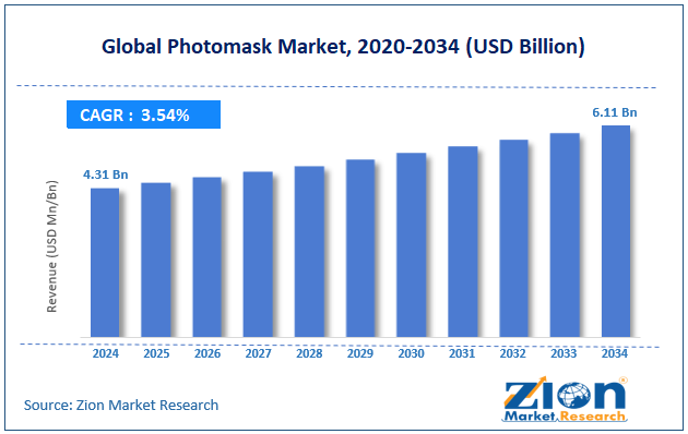
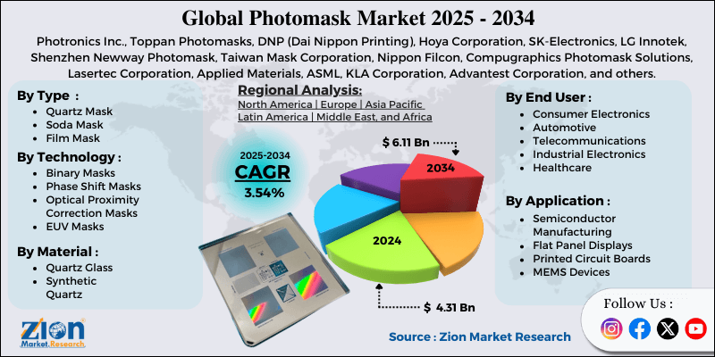
The global photomask market size was worth approximately USD 4.31 billion in 2024 and is projected to grow to around USD 6.11 billion by 2034, with a compound annual growth rate (CAGR) of roughly 3.54% between 2025 and 2034.
Key Insights:
- As per the analysis shared by our research analyst, the global photomask market is estimated to grow annually at a CAGR of around 3.54% over the forecast period (2025-2034).
- In terms of revenue, the global photomask market size was valued at approximately USD 4.31 billion in 2024 and is projected to reach USD 6.11 billion by 2034.
- The photomask market is projected to grow significantly due to increasing semiconductor demand, advancement in chip miniaturization, growing adoption of advanced packaging technologies, expanding flat panel display production, and rising investments in semiconductor manufacturing facilities.
- Based on type, the quartz mask segment is expected to lead the photomask market, while the EUV mask segment is anticipated to experience significant growth.
- Based on technology, the phase shift masks segment is expected to lead the market, while the EUV masks segment is anticipated to witness notable growth.
- Based on application, the semiconductor manufacturing segment is the dominating segment, while the flat panel displays segment is projected to witness sizeable revenue over the forecast period.
- Based on end-use industry, the consumer electronics segment is expected to lead the market compared to the automotive segment.
- Based on the material, the quartz glass segment is expected to lead compared to the synthetic quartz segment.
- Based on region, the Asia Pacific is projected to dominate the global photomask market during the estimated period, followed by North America.
Photomask Market: Overview
A photomask is a highly precise template used in semiconductor manufacturing to transfer detailed circuit patterns onto silicon wafers through a process called photolithography. It works like a stencil with transparent and opaque sections that control the passage of light during chip production. The manufacturing process begins when engineers convert integrated circuit designs into detailed patterns placed on a quartz or glass substrate coated with chromium or other opaque materials. Laser or electron beam systems create these patterns with nanometer-level accuracy, forming features much smaller than a human hair. During semiconductor fabrication, ultraviolet light passes through the photomask and onto a photosensitive chemical layer on the silicon wafer to transfer the pattern. Multiple photomasks are used to build a complete chip, with each mask representing a different layer of the circuit, such as transistors, connections, insulation, and metal interconnects. These masks must maintain extraordinary precision because modern chips contain billions of transistors arranged in extremely small spaces. Any defect or inaccuracy in the mask is repeated on every chip produced, which can damage entire batches and result in large financial losses. The overall quality and precision of photomasks directly influence chip performance, power consumption, and manufacturing yield.
The accelerating demand for advanced semiconductors driven by artificial intelligence, 5G networks, and electric vehicles is expected to fuel substantial growth in the photomask market throughout the forecast period.
Photomask Market Dynamics
Growth Drivers
How is semiconductor miniaturization driving the photomask market expansion?
The photomask market is growing quickly because semiconductor companies aim for smaller transistors and denser chips to meet rising performance needs across artificial intelligence, smartphones, and data centers. Each new chip generation requires more advanced photomasks with finer feature resolution and tighter production precision. Moving from 7 nanometers to 5 nanometers and then 3 nanometer chip production demands completely new mask sets with advanced patterning methods. Extreme ultraviolet lithography supports the smallest features but requires specialized photomasks, which have significantly higher production costs compared to older options. Multiple patterning methods used at smaller nodes require additional mask layers, increasing the number of mask layers used per chip design. Complex three-dimensional structures like FinFETs and gate-all-around transistors need more detailed masks with precise layer alignment.
Advanced packaging methods, such as chiplets and heterogeneous integration, introduce new mask needs for interposer and substrate production. Smaller transistors offer lower power use, higher speed, and reduced cost per function, even with high development expenses. Growing expectations for better cameras, longer battery life, and faster processing increase demand for advanced chips. Artificial intelligence requires huge computational power delivered efficiently by leading semiconductors.
Growing investments in semiconductor fabrication capacity
The global photomask market is growing quickly because governments and companies are investing large amounts of money in new semiconductor manufacturing facilities to reduce chip shortages and limit dependence on a few key production regions. The United States, Europe, China, Japan, and India have announced major plans to build domestic chip production capacity. Each new fabrication facility needs a complete set of photomasks for every chip design it produces. Leading-edge facilities are extremely expensive to build and operate, and photomask production remains a critical component of the supply chain. Geopolitical tensions push countries to secure semiconductor supplies for defense, telecommunications, and critical infrastructure. Pandemic-related chip shortages exposed weak supply chains and encouraged diversification efforts.
Automotive industry disruptions caused by chip shortages led to increased investments in regional production capacity. Government subsidy programs such as the CHIPS Act in America and the European Chips Act lower financial barriers for facility construction. Existing facilities regularly upgrade equipment and expand capacity to support rising demand. Mature node production for automotive, industrial, and consumer products requires steady photomask use alongside advanced node manufacturing.
Restraints
How are high manufacturing costs and complexity creating key restraints for the photomask market?
The photomask industry faces major challenges because manufacturing involves extremely high costs and significant technical complexity, which limits market access and slows adoption of new technologies. Extreme ultraviolet masks cost several hundred thousand dollars each, while complete mask sets for advanced chips exceed many millions. Mask production uses specialized facilities with ultra-clean environments, much cleaner than semiconductor fabrication spaces, as microscopic contamination can easily destroy masks. Advanced pattern-writing equipment based on electron beams or laser systems requires very large capital investments. Mask blank materials must meet strict requirements for flatness, transparency, and uniformity across the entire surface. Inspection systems capable of finding nanometer-scale defects cost millions and need highly trained operators.
Long production lead times, lasting several weeks or several months, create supply chain pressure for urgent chip projects. Complex chip designs increase mask-making difficulty and raise the chances of errors during production. Correcting defects in advanced masks remains extremely difficult and often impossible, which forces complete remakes. A limited number of qualified mask shops worldwide concentrate production in only a few regions.
Opportunities
Expansion of advanced packaging and heterogeneous integration
The photomask industry is gaining strong opportunities because semiconductor manufacturers are using advanced packaging methods that combine multiple chips into single packages for better performance and improved functionality. Chiplet architectures divide complex processors into smaller parts, which are made separately and then assembled. This process requires masks for interposer layers and connection structures. Silicon photonics integration, which links optical and electronic functions, needs highly specialized masks. Three-dimensional stacking places memory chips directly above processors, which demands precise alignment and new mask types. Fan-out wafer-level packaging creates fine redistribution layers that depend on high-resolution masks. System-in-package methods combine different semiconductor technologies such as logic, memory, sensors, and radio frequency components. Advanced substrates with embedded components use mask sets for subtractive and additive manufacturing steps.
Micro-LED displays for augmented reality and premium screens require extremely precise patterning masks. Power electronics built with wide-bandgap materials such as silicon carbide and gallium nitride need masks optimized for different material behaviors. Flexible electronics and printed sensors introduce new application areas for mask producers. Biotechnology applications, including DNA sequencing and medical diagnostics, use microfluidic devices produced with photomask techniques.
Challenges
How are supply chain constraints and geopolitical factors affecting the photomask market?
The photomask market faces significant challenges due to the concentration of production capacity, complex supply chains, and geopolitical tensions that threaten the reliability of supply and access to technology for global chip manufacturers. Most advanced photomasks come from facilities in Taiwan, South Korea, Japan, and the United States, creating a serious risk during regional disruptions. Natural disasters, political instability, or conflicts could interrupt supplies to companies across the world. Export controls on advanced semiconductor technologies restrict the movement of photomask equipment and materials between countries. Intellectual property theft concerns reduce international cooperation on mask design work. Trade restrictions complicate cross-border mask shipments that require special licenses and detailed inspections.
Raw material sourcing for mask blanks and pellicles depends on a few suppliers that are vulnerable to disruption. Specialized chemicals and gases used in mask production often face supply limits during peak demand. Equipment manufacturers for mask-writing systems are concentrated in the Netherlands, Japan, and the United States, with long delivery times. Skilled workforce shortages in design, production, and inspection slow capacity expansion.
Photomask Market: Report Scope
| Report Attributes | Report Details |
|---|---|
| Report Name | Photomask Market |
| Market Size in 2024 | USD 4.31 Billion |
| Market Forecast in 2034 | USD 6.11 Billion |
| Growth Rate | CAGR of 3.54% |
| Number of Pages | 214 |
| Key Companies Covered | Photronics Inc., Toppan Photomasks, DNP (Dai Nippon Printing), Hoya Corporation, SK-Electronics, LG Innotek, Shenzhen Newway Photomask, Taiwan Mask Corporation, Nippon Filcon, Compugraphics Photomask Solutions, Lasertec Corporation, Applied Materials, ASML, KLA Corporation, Advantest Corporation, and others. |
| Segments Covered | By Type, By Technology, By Application, By End Use Industry, By Material, and By Region |
| Regions Covered | North America, Europe, Asia Pacific (APAC), Latin America, Middle East, and Africa (MEA) |
| Base Year | 2024 |
| Historical Year | 2019 to 2023 |
| Forecast Year | 2025 - 2034 |
| Customization Scope | Avail customized purchase options to meet your exact research needs. Request For Customization |
Photomask Market: Segmentation
The global photomask market is segmented based on type, technology, application, end-use industry, resolution, material, substrate size, and region.
Based on type, the global photomask industry is classified into quartz masks, soda masks, film masks, and others. Quartz mask leads the market due to its superior optical properties, thermal stability, and dimensional accuracy, which are required for advanced semiconductor manufacturing at small feature sizes.
Based on technology, the industry is segregated into binary masks, phase shift masks, optical proximity correction masks, and EUV masks. Phase shift masks lead the market due to their ability to improve resolution and image quality for sub-wavelength features in advanced chip production.
Based on application, the global photomask market is divided into semiconductor manufacturing, flat panel displays, printed circuit boards, and MEMS devices. Semiconductor manufacturing is expected to lead the market during the forecast period due to the massive chip production volumes and continuous technology advancement requiring new masks.
Based on end-use industry, the global market is segmented into consumer electronics, automotive, telecommunications, industrial electronics, and healthcare. Consumer electronics hold the largest market share due to the enormous production of smartphones, computers, and entertainment devices, which drives semiconductor demand.
Based on material, the global market is segmented into quartz glass, synthetic quartz, and others. Quartz glass holds the largest market share due to excellent transparency, low thermal expansion, and proven reliability for critical semiconductor applications.
Photomask Market: Regional Analysis
Asia Pacific leads due to concentrated semiconductor manufacturing.
Asia Pacific holds a leading place in the photomask market because the region produces most of the world’s semiconductors and electronic components across many large manufacturing hubs. Taiwan, South Korea, and China dominate chip production with huge fabrication facilities operated by major foundries and integrated device manufacturers across multiple technology nodes. Taiwan Semiconductor Manufacturing Company produces a very large share of global chips, creating extremely high photomask demand across many product lines. South Korean memory companies supply most global DRAM and NAND flash, requiring steady mask deliveries for continuous production. Chinese semiconductor expansion supported by government programs increases mask needs despite technology limitations. Japan maintains strong roles in mature node production, power devices, and specialized semiconductor products across important industries. Regional mask shops support local fabrication facilities with fast turnaround and strong technical assistance across many projects.
Established supply chains connect mask makers, material suppliers, and chip producers efficiently through long-term partnerships. Lower production costs compared to Western countries support regional competitiveness across manufacturing operations. Government policies encourage semiconductor growth through subsidies and infrastructure development across major technology zones. Large electronics clusters create concentrated demand across consumer and industrial sectors.
What is driving North America's steady growth in the photomask market?
North America is experiencing steady growth in the photomask market, driven by the expansion of domestic semiconductor manufacturing through new facility construction and upgrades, supported by government incentives and supply chain security priorities. The CHIPS and Science Act provides major funding for semiconductor manufacturing in the United States and encourages the construction of several advanced fabrication facilities across multiple states. Intel, Samsung, and TSMC are building large facilities in Arizona, Texas, and New York, requiring complete photomask supply chains for many chip designs.
Existing fabrications in Oregon, California, and New Mexico continue moving toward advanced nodes through major equipment upgrades. Strong presence of fabless chip designers, including Qualcomm, NVIDIA, and AMD, creates a rising demand for advanced masks used in leading semiconductor products. Major mask shops in California and Texas serve domestic and international customers across many technology levels.
Advanced research institutions work with industry on next-generation lithography and mask technologies across key development programs. Defense and aerospace sectors require secure domestic mask production for sensitive applications. Automotive industry growth in electric vehicles and autonomous driving increases semiconductor use per vehicle. Data center expansion by cloud computing companies raises demand for processors and memory chips across large installations.
Recent Market Developments:
- In August 2025, Tekscend Photomask announced it is targeting a valuation of about ¥300 billion (≈ US$2 billion) for its upcoming IPO on the Tokyo Stock Exchange, reflecting strong growth expectations in photomask production.
- In August 2025, Photronics Inc. deployed its first U.S. merchant multi-beam mask writer in Boise, Idaho, supporting domestic demand for 3 nm/2 nm node photomasks and aligning with the goals of the CHIPS and Science Act.
Photomask Market: Competitive Analysis
The leading players in the global photomask market are:
- Photronics Inc.
- Toppan Photomasks
- DNP (Dai Nippon Printing)
- Hoya Corporation
- SK-Electronics
- LG Innotek
- Shenzhen Newway Photomask
- Taiwan Mask Corporation
- Nippon Filcon
- Compugraphics Photomask Solutions
- Lasertec Corporation
- Applied Materials
- ASML
- KLA Corporation
- Advantest Corporation
The global photomask market is segmented as follows:
By Type
- Quartz Mask
- Soda Mask
- Film Mask
- Others
By Technology
- Binary Masks
- Phase Shift Masks
- Optical Proximity Correction Masks
- EUV Masks
By Application
- Semiconductor Manufacturing
- Flat Panel Displays
- Printed Circuit Boards
- MEMS Devices
By End Use Industry
- Consumer Electronics
- Automotive
- Telecommunications
- Industrial Electronics
- Healthcare
By Material
- Quartz Glass
- Synthetic Quartz
- Others
By Region
- North America
- The U.S.
- Canada
- Europe
- France
- The UK
- Spain
- Germany
- Italy
- Rest of Europe
- Asia Pacific
- China
- Japan
- India
- South Korea
- Southeast Asia
- Rest of Asia Pacific
- Latin America
- Brazil
- Mexico
- Rest of Latin America
- Middle East & Africa
- GCC
- South Africa
- Rest of Middle East & Africa
Table Of Content
Methodology
FrequentlyAsked Questions
HappyClients