
The Semiconductor Fabrication Material Market is expected to reach a CAGR of 6.5% during the forecast period
04-Dec-2025 | Zion Market Research
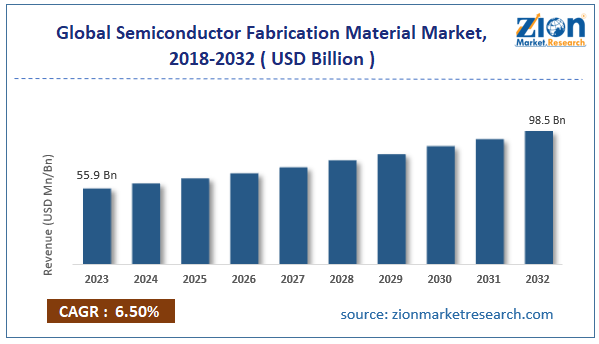
The global semiconductor fabrication material market size was worth around USD 55.9 billion in 2023 and is predicted to grow to around USD 98.5 billion by 2032 with a compound annual growth rate (CAGR) of roughly 6.5% between 2025 and 2034.
Semiconductor fabrication materials are substances used to make microchips, helping create the tiny circuits that power electronic devices. These materials include silicon wafers used as the base, photoresists used to transfer circuit patterns, polishing slurries used to smooth surfaces, etchants used to remove extra layers, and special gases used for coating and cleaning. Chip production needs extremely pure materials, often above 99.999 percent, because even very small impurities can damage circuits or affect performance. Different steps in manufacturing use materials such as polysilicon for gate parts, metals like copper and aluminum for connections, dielectric materials for insulation, and wet chemicals for cleaning. As chip designs become smaller and more complex, material quality requirements become stricter for particle size and chemical makeup. Modern chip factories may use hundreds of materials, each tested carefully for reliable performance. Continuous miniaturization toward advanced nodes push ongoing material innovation.
Browse the full “Semiconductor Fabrication Material Market By Material (Silicon Wafers, Photomasks, Photoresists, Wet Chemicals, CMP Slurry and Pads, Gases, Sputter Targets, and Photoresist Ancillaries), By Application (Consumer Appliances, Power Generation, Electronic Components, and Others), By Industry Vertical (Telecommunication, Energy, Electrical & Electronics, Medical & Healthcare, Automotive, and Others), and By Region - Global and Regional Industry Overview, Market Intelligence, Comprehensive Analysis, Historical Data, and Forecasts 2024 - 2032” Report at https://www.zionmarketresearch.com/report/semiconductor-fabrication-material-market
The semiconductor fabrication material market growth is primarily driven by expanding consumer electronics production and the global push toward advanced manufacturing nodes requiring specialized high-purity materials.
Market Growth Factors
Several factors are propelling the expansion of the semiconductor fabrication material market.
- 5G network deployment: Expansion of fifth-generation wireless systems increases demand for radio frequency chips, baseband processors, and network semiconductors, creating much higher use of fabrication materials across many chip types.
- Electric vehicle adoption: Rising electric vehicle production raises semiconductor use per vehicle because these models need power control chips, battery management systems, sensor processors, and components for autonomous driving functions.
- Artificial intelligence chip demand: Growth in machine learning and artificial intelligence increases the need for specialized processors using advanced packaging materials, strong interconnects, and materials that support complex three-dimensional chip designs.
Restraints
- Raw material supply constraints: Key fabrication materials rely on limited sources of rare earth elements and specialty chemicals, creating risk from supply shortages, political tensions, and price changes for manufacturers.
- Environmental compliance costs: Chip manufacturing uses hazardous chemicals that require costly waste treatment, strict handling steps, and environmental controls, increasing expenses in regions with strict environmental rules.
Semiconductor Fabrication Material Market: Report Scope
| Report Attributes | Report Details |
|---|---|
| Report Name | Semiconductor Fabrication Material Market |
| Market Size in 2023 | USD 55.9 Billion |
| Market Forecast in 2032 | USD 98.5 Billion |
| Growth Rate | CAGR of 6.5% |
| Number of Pages | 221 |
| Key Companies Covered | JSR Corporation, Alent Plc, BASF SE, Air Liquide SA, Praxair Inc., Dow Chemical Company, Air Products and Chemicals Inc., Kanto Chemical Co. Inc., Linde AG, Taiyo Nippon Sanso, and others. |
| Segments Covered | By Material, By Application, By Industry Vertical, and By Region |
| Regions Covered | North America, Europe, Asia Pacific (APAC), Latin America, Middle East, and Africa (MEA) |
| Base Year | 2023 |
| Historical Year | 2018 to 2022 |
| Forecast Year | 2024 - 2032 |
| Customization Scope | Avail customized purchase options to meet your exact research needs. Request For Customization |
Market Segmentation
The semiconductor fabrication material market can be segmented by material type, application, wafer size, technology node, and region.
Based on material type, the semiconductor fabrication material industry is segregated into silicon wafers, photoresists and ancillaries, process chemicals, electronic gases, chemical mechanical polishing materials, and interconnect materials. Silicon wafers are expected to maintain a significant market share during the forecast period due to their fundamental role as the substrate for nearly all semiconductor devices.
Based on application, the semiconductor fabrication material market is divided into memory chips, logic chips, analog chips, discrete devices, and optoelectronics. Logic chips are expected to lead the market during the forecast period due to their use in processors, graphics cards, and application-specific integrated circuits across diverse electronics.
Based on wafer size, the market is segmented into 150 millimeter wafers, 200 millimeter wafers, 300 millimeter wafers, and emerging 450 millimeter formats. 300 millimeter wafers lead the market due to their cost efficiency for high-volume production and widespread adoption across major fabrication facilities.
Based on the technology node, the semiconductor fabrication material market is categorized into above 22 nanometers, 16 to 22 nanometers, 10 to 16 nanometers, 7 to 10 nanometers, and below 7 nanometers. Below 7 nanometers is expected to show strong growth due to performance demands in smartphones, high-performance computing, and advanced applications.
Asia Pacific leads the semiconductor fabrication material market because it contains the largest number of chip manufacturing plants and advanced foundries in the world. Countries such as Taiwan, South Korea, China, and Japan run major facilities that produce chips for global electronics companies and automotive brands. The region benefits from strong supply chains linking material suppliers and chip makers located close to one another. Large government investments support semiconductor growth through subsidies, research programs, and infrastructure aimed at improving regional technological capability. Taiwan Semiconductor Manufacturing Company and Samsung Electronics operate advanced facilities that require highly specialized materials for leading-edge chip nodes.
China’s effort to build domestic semiconductor strength increases investment in new fabrication plants and raises material demand across the region. Lower manufacturing costs and large numbers of trained technical workers support efficient fabrication activity. The strong presence of material suppliers and chemical companies ensures dependable supply chains and technical assistance for manufacturers.
Key Market Players
Leading companies operating in the global semiconductor fabrication material market include:
- JSR Corporation
- Alent Plc
- BASF SE
- Air Liquide SA
- Praxair Inc.
- Dow Chemical Company
- Air Products and Chemicals Inc.
- Kanto Chemical Co. Inc.
- Linde AG
- Taiyo Nippon Sanso
Recent Developments
- In September 2025, JSR Corporation and Lam Research entered a cross-licensing and collaboration agreement to advance next-generation semiconductor manufacturing. The collaboration focuses on dry-resist technology for extreme ultraviolet (EUV) lithography and the development of metal-oxide photoresists and other advanced patterning materials for leading-edge chips.
The global semiconductor fabrication material market is segmented as follows:
By Material
- Silicon Wafers
- Photomasks
- Photoresists
- Wet Chemicals
- CMP Slurry and Pads
- Gases
- Sputter Targets
- Photoresist Ancillaries
By Application
- Consumer Appliances
- Power Generation
- Electronic Components
- Others
By Industry Vertical
- Telecommunication
- Energy
- Electrical and Electronics
- Medical and Healthcare
- Automotive
- Others
By Region
- North America
- The U.S.
- Canada
- Europe
- France
- The UK
- Spain
- Germany
- Italy
- Rest of Europe
- Asia Pacific
- China
- Japan
- India
- South Korea
- Southeast Asia
- Rest of Asia Pacific
- Latin America
- Brazil
- Mexico
- Rest of Latin America
- Middle East & Africa
- GCC
- South Africa
- Rest of Middle East & Africa
About Us:
Zion Market Research is an obligated company. We create futuristic, cutting-edge, informative reports ranging from industry reports, the company reports to country reports. We provide our clients not only with market statistics unveiled by avowed private publishers and public organizations but also with vogue and newest industry reports along with pre-eminent and niche company profiles. Our database of market research reports comprises a wide variety of reports from cardinal industries. Our database is been updated constantly in order to fulfill our clients with prompt and direct online access to our database. Keeping in mind the client’s needs, we have included expert insights on global industries, products, and market trends in this database. Last but not the least, we make it our duty to ensure the success of clients connected to us—after all—if you do well, a little of the light shines on us.
Contact Us:
Zion Market Research
244 Fifth Avenue, Suite N202
New York, 10001, United States
Tel: +49-322 210 92714
USA/Canada Toll-Free No.1-855-465-4651
Email: sales@zionmarketresearch.com
Website: https://www.zionmarketresearch.com